NXP Module 4: Space Vector Modulation
Local Backup
INTRODUCTION
- In this module of the 3-Phase PMSM Control Workshop with NXP's Model-Based Design Toolbox, the focus is on the Space Vector Modulation (SVM) technique needed for generating the appropriate PWM commands for the 3-phase inverter used for controlling the speed and position of PMSM's rotor.
- The goal of this article is to explain step-by-step all the aspects related with power conversion from DC bus voltage to AC phase voltages that are fed to motor windings and cause the motor to spin.
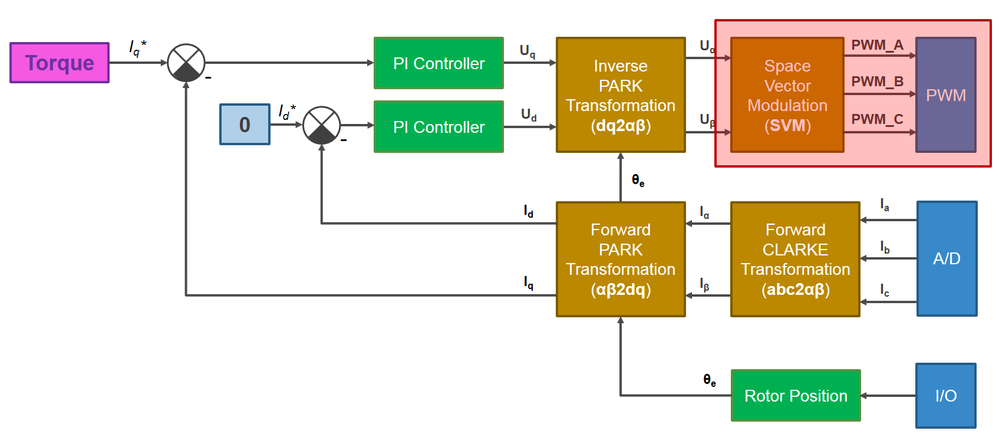
- So far in Module 2: PMSM and FOC Theory and Module 3: System Partitioning we have discussed about Field Oriented Control (FOC) as the main control structure for generating the control quantities that drives the rotor in any position we want. Now, in this module we will focus on methods to convert the digital information provided by FOC into actual voltages that can be applied to the PMSM windings as highlighted in Fig. 1.
- Video training: How To Use Space Vector Modulation (SVM) to Control a PMSM
- Please watch this video before going further. The rest of the article is a summary of the video.
COMMUTATION USED FOR PMSM
- In case of PMSM that are controlled with Field Oriented Control, all three phase windings can conduct current at all times. The only constraint is that the sum of all phase currents must NULL, or putted in other words, the phase currents should form an isolated symmetric 3-phase system.
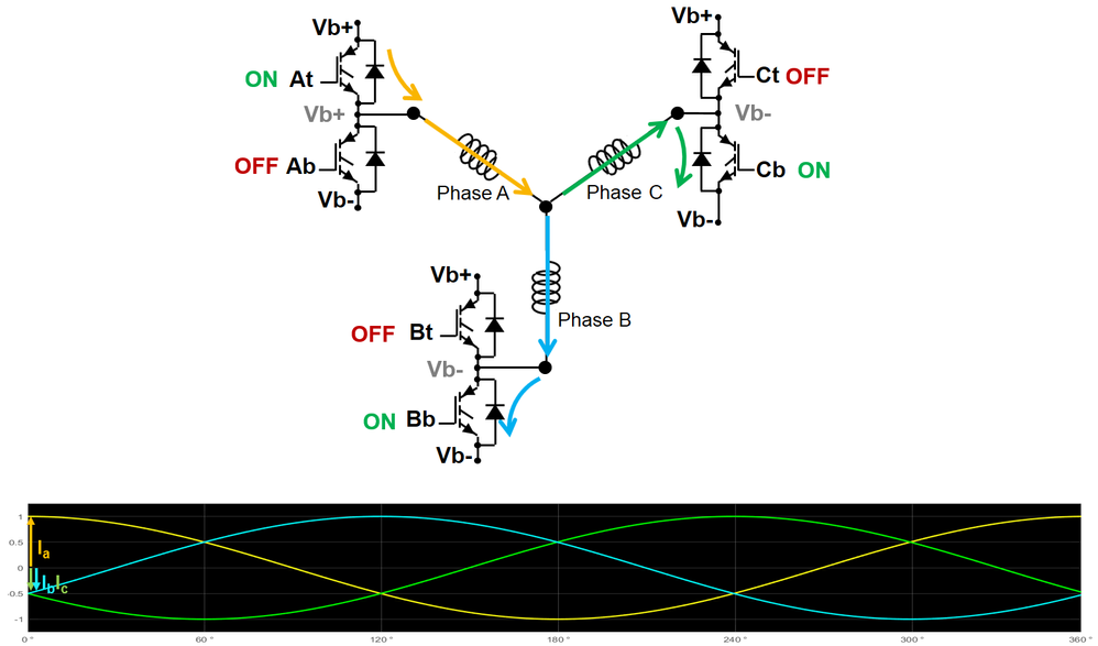
- Using three pairs of switches connected to a voltage source, we can control the current's flow and the magnitude by switching ON or OFF the transistors as shown in Fig 2. The selection of switches ON/OFF state, will determine the current sense, and the time while the which is connected to actual power source will determine the magnitude of the currents that flow thru the windings.
- Note: when we talk about “switch” we refer to an integrated device that contains one transistor (e.g.: MOSFET, IGBT) and one anti-parallel diode. The role of diode is essential in motor control applications due to the nature of the load: inductive
- Since the load is inductive, there are times when the transistor must be turned ON while the current flows in the opposite direction. Since the MOSFET can carry only positive current (from drain to source), the diodes give a path for the current to flow. Without the diode the inductive current with stop instantly, generating high voltage peaks that may damage the transistor.
- To control a PMSM we will need 6 switches that needs to be connected in pairs of two: one connected to a positive voltage source (we call that the TOP switch) and the other one connected to a negative voltage (we call this one the BOTTOM switch).
Each pair of switches will be controlled in complementary mode – meaning the switches can’t be ON in the same time. In general as a precaution, to avoid any accident like short-circuit, there is a small period of time referred as dead-time when both transistors are OFF.
BIPOLAR vs. UNIPOLAR MODULATION
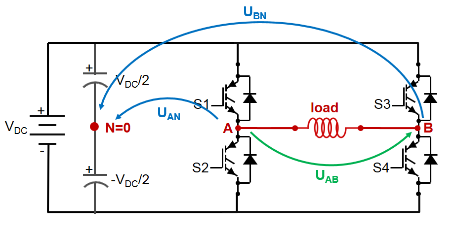
- Lets start with a simple use-case: the single-phase inverter as the one shown in Fig. 3. In general, to control the voltage applied on an inductive load, a single phase inverter made up of 2 pairs of switches (also referred as legs) is used. The voltage on the load (the green arrow) is defined based on the Kirchhoff circuit law as the difference of terminal voltages.
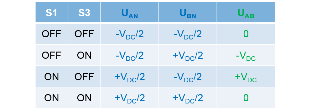
- Since we have four switches, we will have four possible combinations of those and three possible values for the voltage applied on the load as shown in Table 1.
- Depending on how we choose to control the switches, we can have two types of PWM modulations:
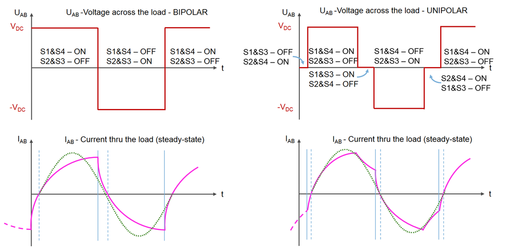
- BIPOLAR – we use only rows 2 and 3 in Table 1 to control the switches. In this case the voltage applied on the load can have only 2 distinct values: +Vdc or –Vdc
- UNIPOLAR - we use all four combinations of switches leading us to a load voltage that can have 3 distinct levels: zero, plus or negative DC bus voltage.
- The main differences between BIPOLAR and UNIPOLAR commutations are highlighted in the Fig.4. On the left, we have the load voltage and current variation for bipolar case while on the right hand side we have the same quantities but this time for unipolar commutation method.
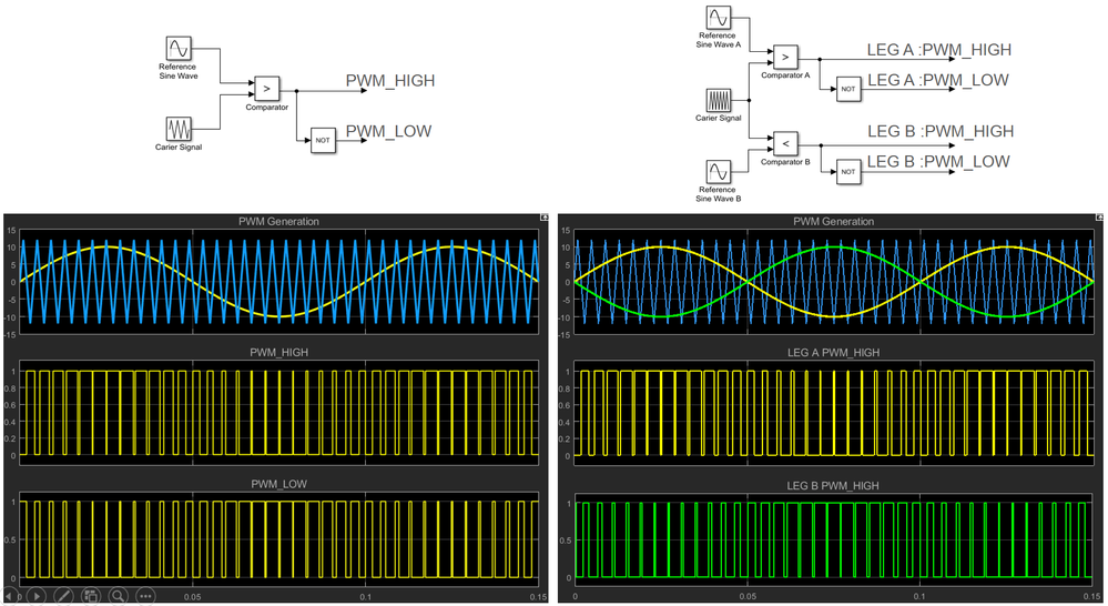
- The bipolar modulation is quite simple and the logic to implement such method is elementary. All we need is a carrier signal, usually a sawtooth signal that is compared against the signal waveform you wish to obtain. The values obtained after comparison are used to control the top and bottom switches that forms one inverter leg. Since the control pulses varies in width – hence the name of Pulse Width Modulation (PWM).
- In case of unipolar modulation, the logic to generate such signals looks similar, the only difference being the fact that we need to add a second reference source to control the switches on the second inverter leg. Usually this second reference signal is phased out with 180 degrees compared with the source for the first inverter leg.
- In Fig. 5, we have an example of switching commands for bipolar (on the left hand side) versus unipolar (on the right side) commutation methods in case of 10 Hz sinusoidal waveform and a 1 kHz carrier signal.
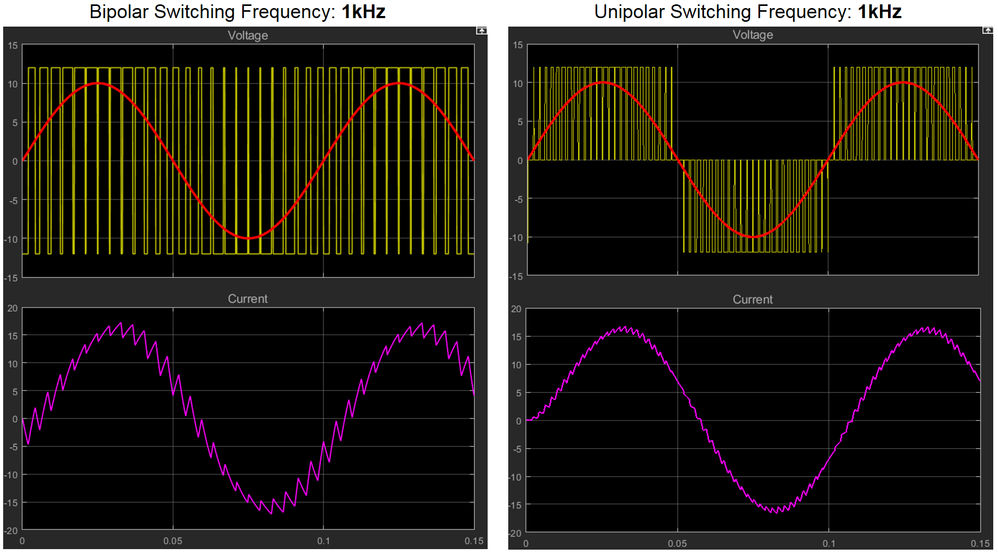
- If we are going to apply these sets of PWM commands to control the voltage and current over an inductive type of load like PMSM windings we are going to obtain the variations shown in Fig. 6. Here you can clearly see the main differences between both commutation methods.
- Note: All these waveform were obtained with Simulink models attached at the end of the article. Feel free to experiment with your own values for R & L
- As we can see there are a few fundamental differences between bipolar and unipolar modulation techniques:
- The first notable difference is the current waveform that is much smoother in case of unipolar commutation than the corresponding one obtained with bipolar modulation. The fact that we apply a smaller effective voltage helps keeping the current ripple smaller and reduces the harmonics produced. As you can seen the current waveform resemble better the sinusoidal waveform in case of the unipolar modulation.
- Less voltage stress seen by the transistors in case of unipolar compared to bipolar method where the transistors needs to switch off 2 times the amount of DC voltage, in unipolar technique they see only half of that stress. This makes the unipolar method more suitable of high-voltage applications.
- The switching logic is more complicated in case of unipolar method since we need to pass thru an intermediate state.
- Effective switching frequency which is higher in case of unipolar commutation even if we used the same 1khz carrier signal.
3-PHASE INVERTER
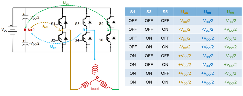
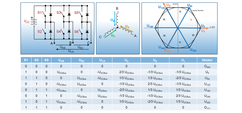
- For PMSM control we will need to use a three leg inverter since we will have three motor terminals that needs to be supplied with power. The inverter is made of six switches that allows eight possible combinations (keep in mind that each pair of switches are controlled in complementary mode: when one is ON the other is OFF)
- If we place a 3-phase symmetric load between the each leg mid-point we can build the Table 2 that summarize the sign and voltage level of each of the switching combinations.
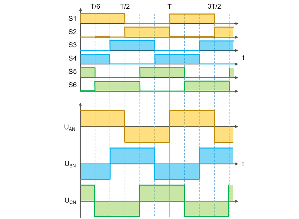
- If Table 2, is confusing to you, lets draw the terminal voltage variation based on the switches gate commands as shown in Fig. 7.
- If we start with a random sequence for top switches commands (ON-OFF-ON), as shown in Table 2 line 6, we see that the voltage sequence will be: positive for terminal A and C and negative for terminal B. Each time we have a top switch in conduction – meaning ON – the terminal voltage will be positive and vice versa when the bottom switch is ON the terminal voltage becomes negative.
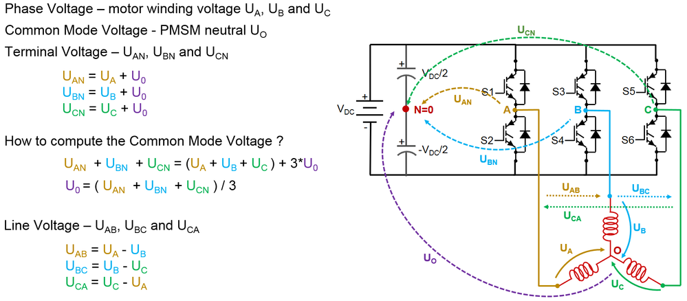
- The Fig. 8 shows the most important quantities we need to measure and control in case of PMSM:
- Phase voltage is the voltage drop on the actual motor windings depicted as Ua, Ub and Uc. In most of the cases there is no way to measure these since you do not have access to the motor internal point where these phases are connected.
- Common mode voltage is defined as the potential between the motor internal phase connection point and the inverter zero potential. Again, this is almost impossible to measure for most of the common used motors.
- Terminal voltage depicted here as Uan, Ubn and Ucn. If we apply Kirchhoff circuit law for voltage then we can derive 3 equations where we see that the terminal voltage is the sum between the motor phase voltage connected to that terminal and the common mode voltage. Knowing the value of the terminal voltage we can easily compute the other 2 quantities: phase voltage and the common mode voltage.
- Line voltage is the voltage between 2 terminals. This is the easiest to be measured since you have easy access to motor or inverter terminals.
SPACE VECTOR MODULATION
- Instead of dealing with each motor phase separately as bipolar of unipolar modulation techniques in Space Vector Modulation (SVM) we are going to treat the three-phase PWM generation as a single task. Instead of generating three independent switching waveforms, we shall consider the three-phase inverter as one unit that can generate eight different switching states: a 3-dimensional Cartesian product of the two states on phase A, the two states on phase B, and the two states on phase C.
- By combining Table 2 for terminal voltage values with the equations for line and phase voltages we can build Table 3 that covers all 8 possible combinations of switches.
- This way we can build 6 unique vectors that covers all 360 degree circle and 2 additional zero combinations. Two of these states (0,0,0) and (1,1,1) represent zero instantaneous line-to-line voltages, and are often called the “zero” or “null” vectors. The remaining six states represent nonzero vector voltages applied across the motor terminals and splits the circle in 6 sectors.
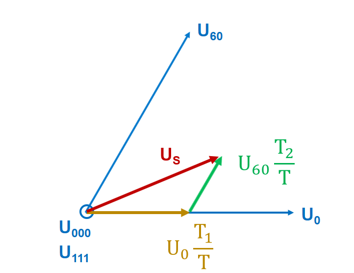
- As depicted in Fig. 9, we can compute any voltage vector magnitude and orientation with just 2 set of commutation sequence and one of the zero vectors.
- Assuming we want to create a new reference voltage vector Us in the first sector that is defined by U0 and U60 we need to:
- know the sampling period T – which is usually set by the switching frequency.
- compute how much time we need to apply the U0 voltage and how much time we need to apply the other vector U60. The T1 and T2 will control the vector orientation and magnitude.
- We start by applying some amount of voltage for some time along one axis, then we move 60 degrees and apply some other amount of voltage and then nothing. Since we change the vectors so fast – much faster than the motor can react – the end result is and average voltage that the motor sees. The motor windings act like an low pass filter smoothing everything.
- The sinusoidal PWM modulation has advantage in its simplicity however does not allow full utilization of DC bus voltage since it allows the phase voltage with maximum amplitude of half of the DC bus voltage. Since the line voltage is defined as phase to phase voltage difference you can easily see that the line voltage is lower than the DC-bus voltage although such voltage can be generated between the terminals.
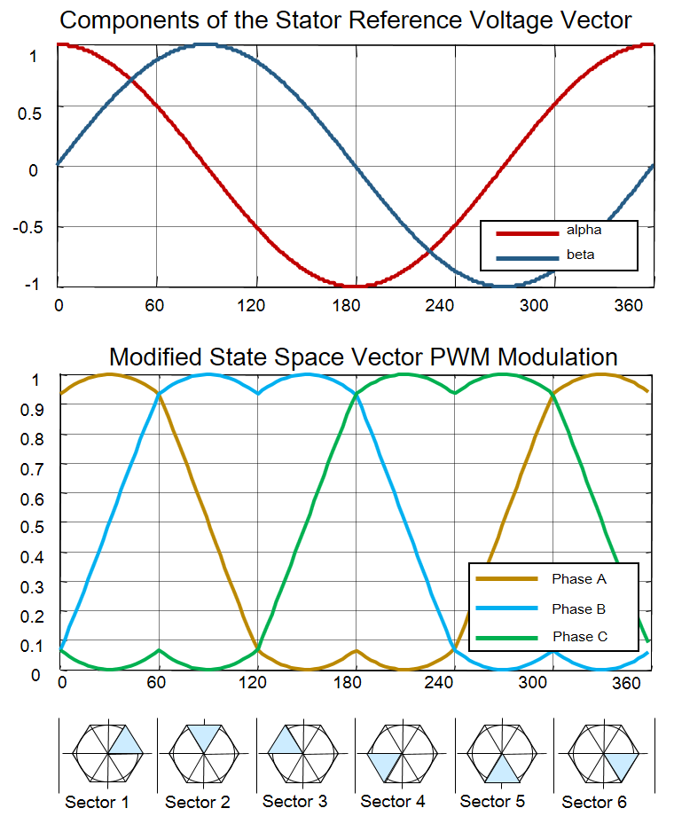
- To overcome this limitation and enhance the motor characteristics of speed and torque we are going to use a Modified Space Vector Modulation that can achieve full DC bus voltage utilization by continuously shifting up and down the 3-phase voltage system. This shifting is called 3rd harmonic injection and allows us to change the amplitude of the phase first harmonic by 15.5% which will allow us to get to higher speed region or deliver higher torque compared to sinusoidal PWM modulation.
CONCLUSIONS
- Using Space Vector Modulation we can translate directly the reference voltage from alpha-beta stationary frame into 3-phase command voltages using a simple approach that considers the inverter a single state machine capable of eight independent states.
- For any voltage vector we want to achieve we can compute three periods that allows us to strictly apply three set of distinct voltages to the motor. The motor will integrate those signals resulting in a unique vector.
- On top of standard SVM we can add the third harmonic injection in order to increase the available voltage available on motor terminals, extending this way the range of motor speed and torque.
- In the next module we will implement and test and application using the practical aspects highlighted in this module.
- We hope you find this information useful. Feel free to LIKE this article and comment below.
Update revisions:
- March 18, 2019
- update the model to work with Model-Based Design Toolbox for MPC57xx Automotive Version 3.0.0.
- May 06, 2020
- update the model to work with Model-Based Design Toolbox for MPC57xx Automotive Version 3.2.0.

